XPS/AES Examples of Activity
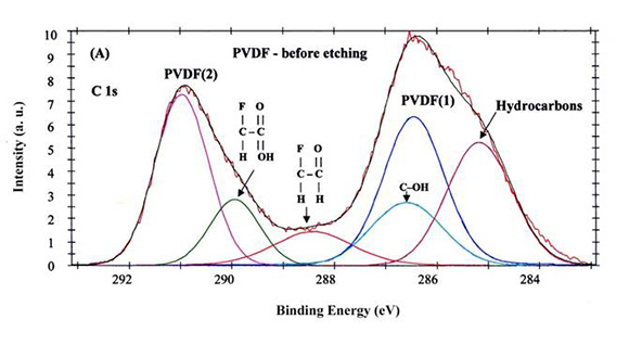
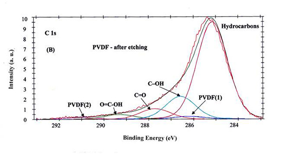
Example #1 (A, B): XPS analysis of the PVDF surface modification.
(A) Plasma processed poly(vinylidene fluoride) (PVDF) before etching:
C 1s signal reveals two typical PVDF peaks, PVDF (1) and PVDF (2), together with hydrocarbon and C-OH contamination. Additional C-F groups are caused by plasma processing.
(B) Plasma processed poly(vinylidene fluoride) (PVDF) after etching in sodium naphthalene: PVDF and plasma-processed structure is screened by the newly appeared C=O, O=C-OH bonding.
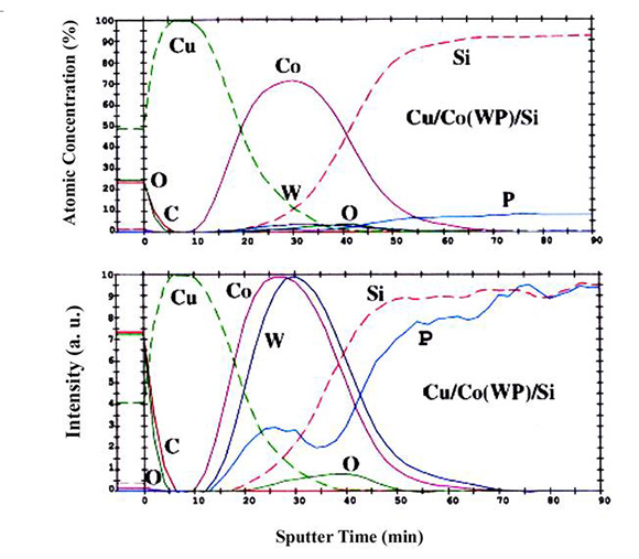
Example #2: XPS investigation of the Co(WP) diffusion barrier for Cu on Si metallization.
XPS depth profile of the Cu/Co(WP)/Si structure demonstrates the role of W in blocking Cu interdiffusion into Si substrate. The upper profile depicts the distribution of the element atomic concentration (A.C. %) with sputter time. The lower one corresponds to the element normalized intensity obtained with sputtering.
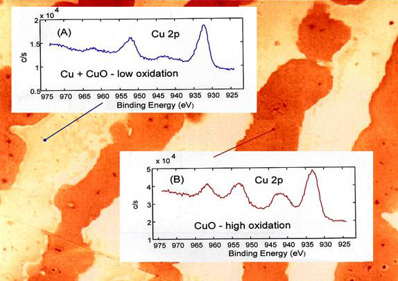
Example #3: XPS investigation of the new technique in developing fingerprints.
The fingerprint is developed in the process of corona discharge. The spectra are superimposed on the SEM image. Cu 2p structure measured on the bare substrate (B) demonstrates a high oxidation as a result of plasma processing. A thin fingerprint layer (A) protects the underlying Cu from strong oxidation. Low Cu oxidation observed in this case is caused by the pores in the fingerprint only. (E. Halahmi, O. Levi, L. Kronik, and R. L. Boxman, J.Forensic Sci. 42, 833 (1997).
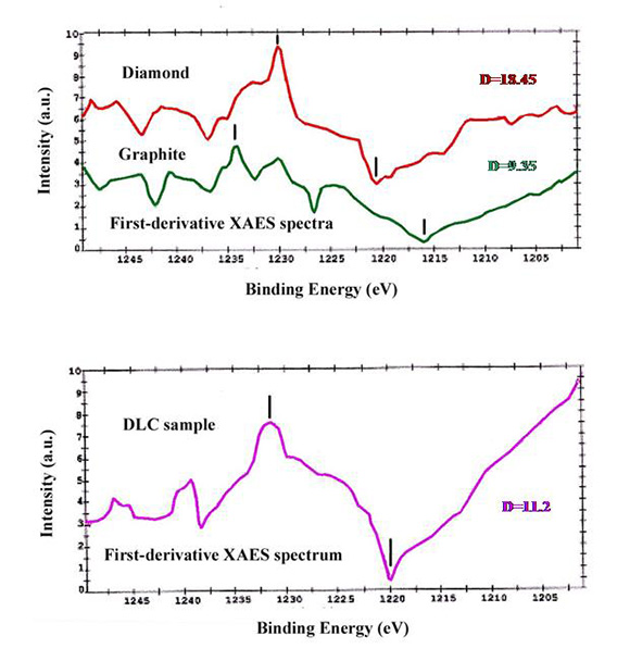
Example #4: Investigation of the DLC processing quality with XAES.
Carbon C KLL Auger transition in graphite, diamond and diamond-like carbon (DLC) samples is measured with high resolution XPS. The row data is smoothed and differentiated for comparing the energy difference between maximum and minimum values (D). D is correlated to the C-C bonding configuration, being sp3 in diamond (D=9.35), sp2 in graphite (D=18.45) and the sp2- sp3 combination in DLC sample (D=11.2).
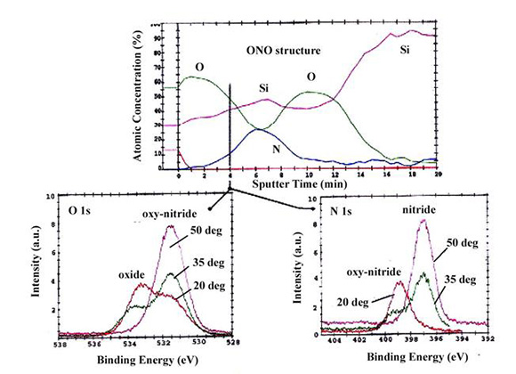
Example #5: ONO structure investigation: depth profiling and high resolution angle resolved XPS (ARXPS) measurements.
ARXPS measurements give a “non-destructive profile” of the sample by collecting the information ranging from the up-most layers (shallow take-off angle) to those situated at a depth of 50-60 Å from the surface. SiO2/Si3N4/SiO2 structure (ONO) grown on Si substrate is characterized by the intermixed interfaces of SixOyNz configuration. The structure is analyzed in 2 steps: first - a regular XPS Depth Profile is measured to reveal an approximate interface position (4 min sputter time), second – high resolution ARXPS measurements are performed on a new sample after 4 min sputtering. ARXPS measurements reveal the exact ONO structure in the close vicinity to the interface.
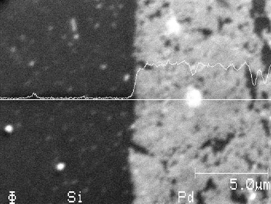
Example #6: Using AES line scan for lateral element distribution analysis.
Pd on Si distribution is presented by plotting Pd line scan on the Pd/Si SEM image.
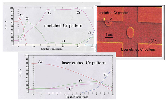
Example #7: Failure analysis.
Colored SEM image reveal two small Cr patterns: before laser etching and after laser etching (marked with black dots). The sample surface is covered with a thin Au layer prior to ion sputtering for charging elimination. AES depth profiles of both patterns are compared. Unetched Cr pattern, taken as a reference, is characterized by a thin oxide layer present at the Cr surface. As follows from the profile of an etched pattern, residual Cr is still left on the surface and is converted by the laser processing into a completely oxidized layer.
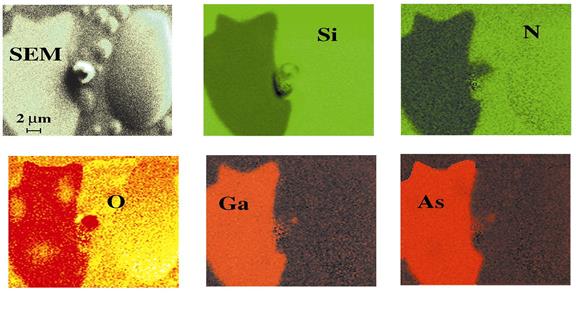
Example #8: AES mapping of the GaAs revealed under the SixNy blister after its bursting.
The colored pictures represent the SEM image (upper, left) and lateral distribution maps of silicon (Si), nitrogen (N), oxygen (O), gallium (Ga) and arsenic (As). SixNy layer, grown upon GaAs substrate, shows blister formation as a result of processing failure. GaAs substrate is revealed under one of the blisters after its bursting.
Explore


