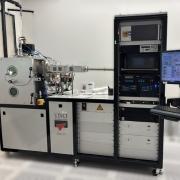
CORIAL ICP-CVD System


The CORIAL ICP-CVD is a High-Density Plasma Chemical Vapor Deposition (ICP-CVD) system designed for the low-temperature deposition of high-quality dielectric, semiconductor, and functional thin films. The system supports a broad range of silicon-based materials, including silicon oxide, silicon nitride, silicon carbide, silicon oxynitride and hydrogenated amorphous silicon. making it an ideal platform for semiconductor fabrication, MEMS, photonics, and advanced materials research.
The Corial ICP-CVD system uses a high-density inductively coupled plasma (ICP) source to remotely ionize precursor gases, keeping the plasma away from the substrate. The ionized species are then gently drawn to the substrate at low energy, minimizing ion bombardment and substrate heating while producing dense, high-quality films. By ICP power and substrate bias can be controlled independently, allowing the plasma density and ion energy at the substrate to be adjusted separately. This provides precise control over film properties while minimizing ion-induced damage and substrate heating.
The system's low-temperature deposition capability makes the CORIAL ICP-CVD ideal for temperature-sensitive substrates and advanced microfabrication processes. Compared with conventional PECVD ICP-CVD can provide high-quality films at lower substrate temperatures, with good film density, low ion damage, controllable mechanical stress, and improved step coverage. These capabilities support deposition over patterned surfaces, trenches, and vias, although achievable conformality depends on the material, process conditions, and feature geometry.
The CORIAL ICP-CVD supports applications in semiconductor fabrication, MEMS, photonics, advanced packaging, and materials research. It can accommodate substrates ranging from 150 mm wafers to small dies and sample pieces, providing a flexible platform for research, prototyping, and low-volume fabrication.
Common Applications:
- Low-temperature thin film deposition
- Conformal coating of complex structures, trenches, and vias
- Surface passivation
- MEMS fabrication
- Photonics and optoelectronic devices
- Microfabrication process development
- Nanotechnology and advanced materials research
Explore